From nanometer‑smooth facets to porous, defect‑rich layers, the choice of wet or dry etch—and every parameter behind it—can make or break device performance. Inline metrology and careful chemistry selection are the guardrails.
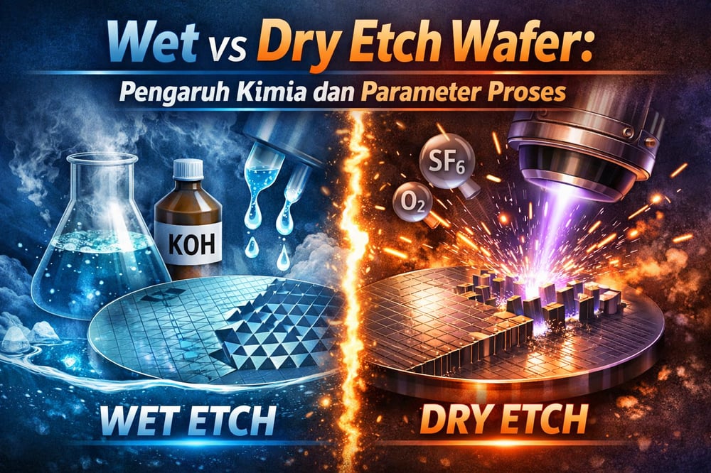
In semiconductor fabs, etch is where surface science turns surgical. Wet chemical solutions versus dry plasmas shape not just profiles but the very chemistry of the wafer surface, with measurable consequences for roughness, defects, and even photocurrent.
One published case quantified this directly in solar cells: a reactive ion etch left an amorphous SiOₓ “damage” layer that increased recombination and cut efficiency; a dilute HF clean to remove it boosted short‑circuit current density by ≈1.6 mA/cm², translating to about a 0.6% absolute efficiency gain (sciencedirect.com; sciencedirect.com).
The through‑line across studies: every etching chemistry and condition leaves a distinctive surface fingerprint that must be selected, tuned, and verified with metrology.
Wet versus dry etch surface outcomes
Wet etches (liquid acids, bases, oxidizers) and dry etches (plasma RIE/ICP; reactive ion etching/inductively coupled plasma) act differently on silicon and its films. Alkaline solutions such as KOH (potassium hydroxide) or TMAH (tetramethylammonium hydroxide) etch silicon anisotropically (direction‑dependent rates along crystal planes), generating crystallographic facets. Acids like HF (hydrofluoric acid) attack oxides and silicon more isotropically (uniform in all directions).
Additives and conditions matter. In a MEMS‑oriented study, Si wafers etched in KOH with 5–10% isopropanol (IPA) produced well‑defined triangular pits on {111} surfaces: without IPA, pit corners were rounded, but at 10% IPA each corner sharpened to ≈60°, giving nearly equilateral triangle cross‑sections (pubs.acs.org; pubs.acs.org). High‑concentration KOH at low temperature (18 M, 40 °C, ~25 nm/min etch rate) produced mirror‑smooth sidewalls (RMS roughness ≈10.8 nm), while faster etches (10 M, 80 °C) generated roughness >50 nm—underscoring that high‑concentration/low‑temperature recipes can yield nanometer‑scale smoothness (researchgate.net).
By contrast, strong oxidizing formulas (HF/H₂O₂, “piranha” H₂SO₄+H₂O₂, HCl/HNO₃, etc.) can roughen surfaces if misused. One cautionary example: HF vapor etching of Si(100) created a porous nanostructure; SEM showed ∼6 nm pores and 4 nm “quantum dot” Si crystallites with visible red luminescence—evidence of defect‑rich material from uncontrolled exposure (scirp.org; scirp.org). In practice, oxide removal is usually done with buffered HF (BOE) to avoid such damage; standard recipes call for HF or BOE to strip native oxides (sensing.matsushima-m-tech.com). Selection also hinges on selectivity: KOH/TMAH does not etch SiO₂, while HF/BOE will aggressively attack oxides but leave Si intact, so the choice must match the layer stack.
Dry plasmas bring directionality and different risks. Highly directional RIE or ICP—e.g., SF₆/CF₄ for silicon and Cl₂/BCl₃ for polysilicon/metals—enable vertical profiles but can implant ion damage or redeposit passivation films. In solar‑cell plasma texturing, an amorphous SiOₓ “damage” layer formed on wafer surfaces, increasing carrier recombination and reducing efficiency; a dilute HF step removed it and recovered performance (Jₛc +≈1.6 mA/cm²; ~0.6% absolute efficiency gain) (sciencedirect.com; sciencedirect.com). Wet chemical texturing (acid etch) of multicrystalline Si is somewhat more uniform but can be sensitive to scribing marks and requires strong oxidizers to attack saw damage (sciencedirect.com).
Parameter control: rate, selectivity, agitation
Etch chemistry and tuning parameters—concentration, temperature, pressure, power—must align with device layers. Etching 200 nm SiO₂ through a polymer mask demands very high oxide:polymer selectivity (>100:1) or the mask erodes; etching silicon under a thin Si₃N₄ mask calls for near‑100:1 Si₃N₄:Si selectivity or the nitride is overconsumed.
In wet benches, controlling KOH or HF concentration and temperature tunes rate and smoothness; slower KOH etches (by cooling or dilution) can dramatically cut roughness (researchgate.net). Small‑percent additives such as IPA or surfactants in TMAH suppress hillock and undercut; IPA has been shown to smooth Si surfaces and steepen facets (pubs.acs.org; pubs.acs.org). A baseline requirement here is accurate chemical dosing, which production lines typically implement with dedicated dosing pumps.
Mechanical factors matter: in KOH etching, H₂ bubbles or soluble products can locally halt etching unless dispersed. Reports emphasize continuous stirring (magnetic or megasonic) to sweep residues (pubs.acs.org). In an optical study, static HF/HNO₃ etching worsened roughness over time, whereas an ultrasonic‑agitated KOH bath left roughness unchanged; the acid mix raised polished‑glass RMS roughness by up to 20× (from ~3 nm to ~50 nm), while KOH with stirring kept it near the original level (the HF mix produced nanoscale digs that strongly scattered light) (opg.optica.org; opg.optica.org).
Damage modes and endpoint control
Process extremes can induce micro‑defects. Fluorocarbon plasma SiO₂ etches can form micro‑trenches or polymeric residue at feature bottoms. Over‑etching photoresist in O₂ plasma can roughen or scorch underlying films. In metals, over‑etch can undercut lines or leave “grass.”
Endpoint strategies—time control or in‑situ tools such as optical emission or interferometry—help avoid overshoot and its characteristic surface damage.
Post‑etch surface metrology toolkit
After etch, metrology confirms that surfaces meet spec. AFM (atomic force microscopy; nanometer‑scale 3D mapping with vertical resolution <1 nm) quantifies roughness; automated AFM systems can even review defects across full 300 mm wafers (magazine.nanoscientific.org). SEM (scanning electron microscopy) resolves sidewalls and profiles; SEM of Si nanogratings confirmed perfectly periodic trenches and verified cross‑section angles (link.springer.com). Laser scanning interferometry (optical profilometry) and confocal microscopy measure large‑area roughness and pit geometry; in KOH/IPA work, confocal laser scanning captured RMS roughness on (100) and (110) planes (researchgate.net).
For thickness and uniformity, ellipsometry or reflectometry tracks depth across the wafer; stylus or optical profilometers verify step heights. For composition, XPS (X‑ray photoelectron spectroscopy) and AES (Auger electron spectroscopy) identify surface chemistry. One fab‑line case used XPS to find Ti–Fₓ bonds on a TiN hardmask left by prior plasma and to confirm their removal after wet cleaning (researchgate.net). In the nanograting work, XPS of cleaned Si patterns showed only Si signals—no oxides or organics—and EDX/SEM mapping showed only Si (no O, C, or metal peaks) on patterned surfaces (link.springer.com; link.springer.com). SIMS (secondary ion mass spectrometry) or RBS (Rutherford backscattering) can profile dopants or detect trace contaminants when needed.
Defect inspection uses laser light‑scattering tools to find particles, digs, and pits; decorative etching can highlight subsurface defects for SEM/AFM review. One automated AFM defect‑review study etched a wafer to reveal crystals and used non‑contact AFM to 3D‑profile each pit, correlating with SEM images (magazine.nanoscientific.org). Quantitative outcomes guide control: in fused silica, KOH etch left RMS roughness essentially unchanged, whereas HF/HNO₃ raised RMS to tens of nanometers (opg.optica.org). In an optical stack, polishing plus a wet KOH/H₂O₂ clean achieved sub‑nm roughness; omitting the clean led to scattering and yield loss (noted by the same interferometry/XPS group).
Optimization tradeoffs and safety controls
Aggressive chemistries (strong HF, hot KOH, plasma) often etch fast but risk wafer damage or equipment corrosion; milder recipes can improve surface quality but may reduce throughput. Integrating H₂O₂ into KOH can raise etch rate (oxidizing Si to a softer oxide) but roughen surfaces at high dose. Adding NH₄F to HF (making BOE) boosts oxide removal but forms (NH₄)₂SiF₆ precipitates that can redeposit; an optics study found BOE must be ultrasonically agitated to avoid haze, whereas HF+HNO₃ could be static (opg.optica.org).
Handling and disposal are tightly regulated. Indonesian technical guidelines specify that HF requires acid‑resistant containers, cool/dark storage, and segregation from incompatible chemicals (sensing.matsushima-m-tech.com). Under Indonesian law, strong etchants (HF, H₂SO₄, etc.) produce B3 (toxic) waste that demands neutralization and licensed disposal (world.moleg.go.kr).
In practice, fabs often combine steps: a “hard etch” to remove bulk material followed by a gentle finishing etch or clean to polish the surface. Inline metrology then checks profile, roughness, %non‑uniformity, and defect density targets after each etch. Published reports indicate that careful parameter control—low etch‑rate strategies (researchgate.net), IPA additives (pubs.acs.org), sufficient agitation (pubs.acs.org)—can reduce roughness by factors of 3–5 or more. These gains translate to better device yield and performance (as seen in the ~0.6% solar efficiency recovery, sciencedirect.com), and to laser damage threshold enhancements from etch‑passivation evidence (opg.optica.org).
Data‑driven selection and verification
Quantitative outcomes—etch rate (nm/min), selectivity, RMS roughness (nm), defect density, film uniformity—are the scoreboard. Combining well‑chosen recipes with real‑time controls (endpoint detection) and post‑etch analysis (SEM/AFM, XPS/EDX, profilometry) ensures the desired material is removed cleanly without compromising the device. That approach is the common thread linking smooth KOH facets, avoided HF‑induced porosity, recovered solar‑cell current, and uniform nanograting surfaces (sources throughout: peer‑reviewed journals, industry reports, and technical papers as cited above).
